Intel's Advanced Manufacturing Facilities in Penang
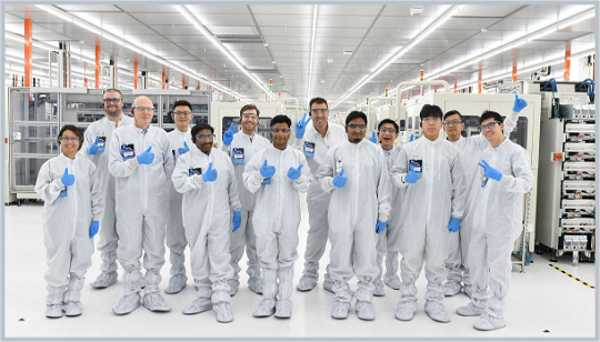
Intel’s most Advanced Manufacturing facilities give a glimpse into the world of chip making. The Intel Fab Tour gives us a look at the fields of science and wizardry that go into manufacturing semiconductors, from cutting and sorting wafers to testing and assembling chips at every stage. The company’s most advanced facilities are in Penang, Malaysia, but you can also find them in other parts of the world, such as Hillsboro, Oregon.
The Penang facilities include areas for cutting and sorting wafers, assembling them onto substrates, and conducting rigorous testing at every stage. Intel’s representatives claim that its manufacturing is the most advanced on the planet. We were able to take a tour of the fab to see the technologies and innovations that make it so.
Intel’s aggressive roadmap, known as IDM 2.0, has the company building resilient supply chains, adopting scalable manufacturing processes, and providing manufacturing expertise to fabless customers. The roadmap includes building technology at five nodes in four years; Intel 7 is already in full production, and Intel 4 is ramping up.
Alongside its manufacturing efforts, Intel sees AI becoming a ubiquitous part of everyday computing. The company aims to create an open ecosystem for AI development, with a particular focus on edge AI and data centre AI.
Wafer Processing, Preparation, and Sorting
We start our tour at the wafer processing area, where wafers are processed, prepared, and sorted before being sent to assembly facilities worldwide. Wafers are cut with precision using laser scribing and mechanical cutting. Amazing sorting machines, weighing 1000 pounds each, test and sort the dies.
Assembly and Test Factory
The assembly and test factory houses the Penang Assembly and Test facility. Incoming dies are assembled onto substrates, a critical part of the chip making process. Chip packaging is an important aspect, especially with modern chiplet designs and 3D stacking technologies. Here is a quick overview of the entire process:
Intel’s fab tour is designed to show off the company’s technology and wizardry. Intel’s aggressive roadmap, which includes building technology at five nodes in four years, and its investments show its determination to catch up to TSMC’s manufacturing leadership. The company’s vision also includes making AI a ubiquitous part of everyday computing, which is why it’s important to have an open ecosystem for its development.


